Proudly representing JTAG Technologies

JTAG Technologies is boundary-scan.

Since the early 1990s they have lived and breathed the technology that has revolutionized the manufacture and test of digital and mixed signal Printed Circuit Board Assemblies (PCBAs) the world over.

JTAG Technologies. We are boundary scan.

JTAG Technologies is and will stay in the heart of electronics. Electronics is everywhere; the world as we know it wouldn’t function without chips and circuit boards. Mobile phones, cars or even hospital beds can only work with those tiny soldered components. But before any chip can start performing, it needs to be tested. That’s where JTAG Technologies comes in, the Eindhoven based company that has taken the manufacturing and testing of digital and mixed signal PCBs to a new level.

Our boundary scan products can be found in design labs and factories in over 50 countries across the globe and have solved or prevented thousands of board test problems. Since 1993 the company has ensured that this outstanding method for verifying designs and testing printed circuit boards during and after production remained up to date.


Throughout the years, its products and services have grown in line with the evolving standards, technological developments and also with the market and the ever changing regulations.

Discover and experience our corporate story.

Different hardware and software products for test and device programming are available for design, production and service. While testing and device programming require different software modules, the same hardware can support both types of applications.

Technology

JTAG/boundary scan, based on IEEE Std 1149.1 and related standards, is now widely used in the electronics manufacturing industry to solve difficult test problems on complex Printed Circuit Board Assemblies (PCBAs). By overcoming the access difficulties which often degrade the efficiency of conventional test methods, boundary scan has become the pre eminent structural test method in the 21st century. This growth has been further helped by improvements in software application tools and increasingly versatile hardware from JTAG/boundary scan tools providers. Besides test there are additional, derivative uses and application environments for boundary scan. This can lead to benefits across a product’s life cycle, not just in manufacturing testing.

Solutions

Throughout the life cycle of your products 
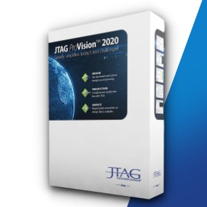
JTAG/boundary scan can be used for testing and device programming. Whether it’s in automotive, healthcare, astronomy, mil aero or other high technology industry, JTAG Technologies helps you achieve the performance that matches your ambitions. And also those of your clients.


By providing tools for each discipline Design, Production and Service we guarantee the best result in every stage of your product lifecycle.

Design

Production

Service

A selection of what our customers say:

JTAG Technologies consistently delivers extremely high quality software tools and their conscientious customer support staff is excellent.

Tim Nolan,

US

Compared with the previous generation of software, we estimated that test development time can be reduced by up to 30% with JTAG ProVision.

Lee Bogardus,

US

In theory, there are alternatives for boundary-scan, but for me, they don’t come close.


Terry Walton,

US

Why use boundary-scan?

  • Reduced time to market
  • Faster ROI
  • Reusable Test Vectors
  • Reduced Test Time
  • Reduced Design Iterations
  • Increased Availability
  • Efficient and Economical Production

Why choose JTAG Technologies?

  • Testing and device programming solutions
  • Solutions for Design, Production and Service
  • One of the primary architects of boundary-scan
  • Customers in more than 50 countries
  • 10.000+ systems sold
  • The number one dedicated boundary-scan company
  • World class, worldwide support